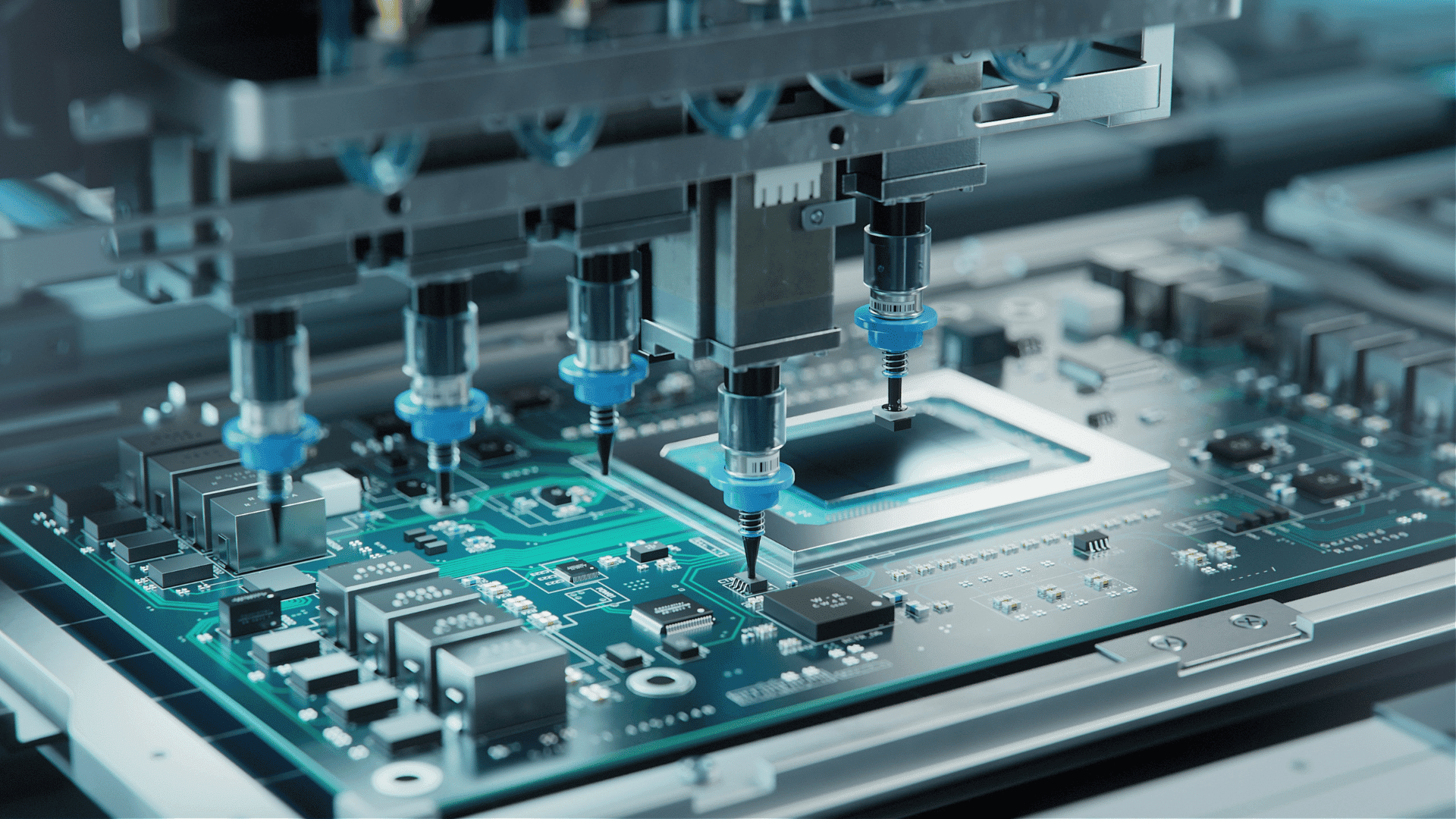
Modern chipmaking is in a unique position for several reasons. For example, as the demand for AI and faster electronics skyrockets, the factories building these chips are facing a massive cleanup challenge. A new review in Environmental Science & Technology points out that the semiconductor industry relies heavily on “forever chemicals,” or PFAS, but doesn’t know how to get rid of them.
These chemicals are used because they can handle the intense heat and chemical reactions needed to etch tiny circuits onto silicon. However, they don’t break down in the environment, which is why they’ve earned their “forever” nickname.
Semiconductor Manufacturing’s Major Problem


The scale of the waste in semiconductor manufacturing is hard to grasp. Large factories can churn through thousands of cubic meters of wastewater every single day.
“Managing the waste from these facilities is a massive undertaking,” said Xiao Su, a professor at the University of Illinois Urbana-Champaign. “A single large factory can produce thousands of cubic meters of wastewater per day, containing a ‘soup’ of diverse PFAS mixed with various solvents, metals and salts.”
Advertisement
Most current tech was built for city tap water, not the complex chemical cocktails found in a semiconductor plant. To make things harder, many of the chemical formulas are trade secrets, so researchers don’t always know exactly what they’re trying to clean up.
Finding a Path Forward
Experts from universities and the tech industry recently had a brainstorming session to find a solution. They focused on tracking the chemicals better, separating them from the water, and eventually destroying them.
One idea involves using AI and high-resolution imaging to see how these chemicals change during the manufacturing process. Researchers are also looking at ways to literally break the chemical bonds using plasma or electricity. However, new tools must fit into a factory that’s already packed with equipment.
“A typical semiconductor fabrication facility could easily have hundreds or even a thousand manufacturing steps, and these are all integrated with each other,” said Devashish Gokhale, a lead co-author of the study. “If you develop new treatment solutions, they need to be able to fit inside this complex operation without affecting everything else that’s highly optimized.”


