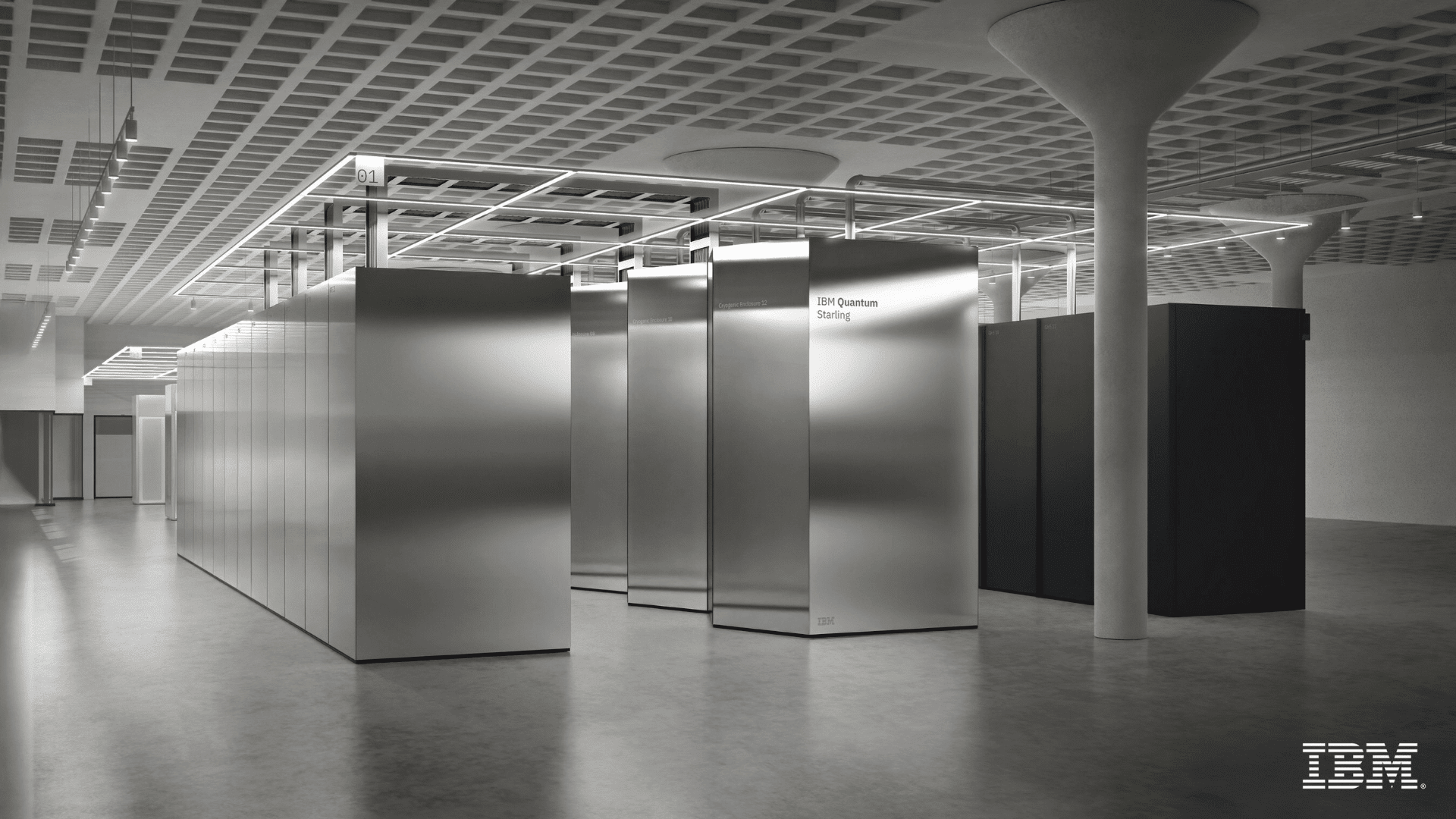
Computers do almost everything we do today. However, the chips within the computers are hitting a physical wall. There is literally no more room to make them smaller. Today, IBM announced a solution to this issue. They created the world’s first sub-1-nanometer chip.
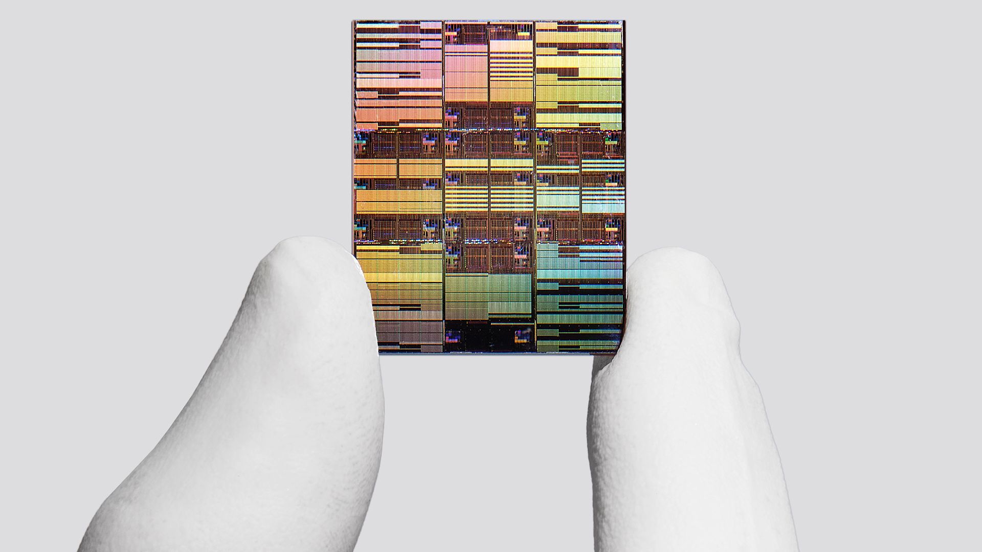
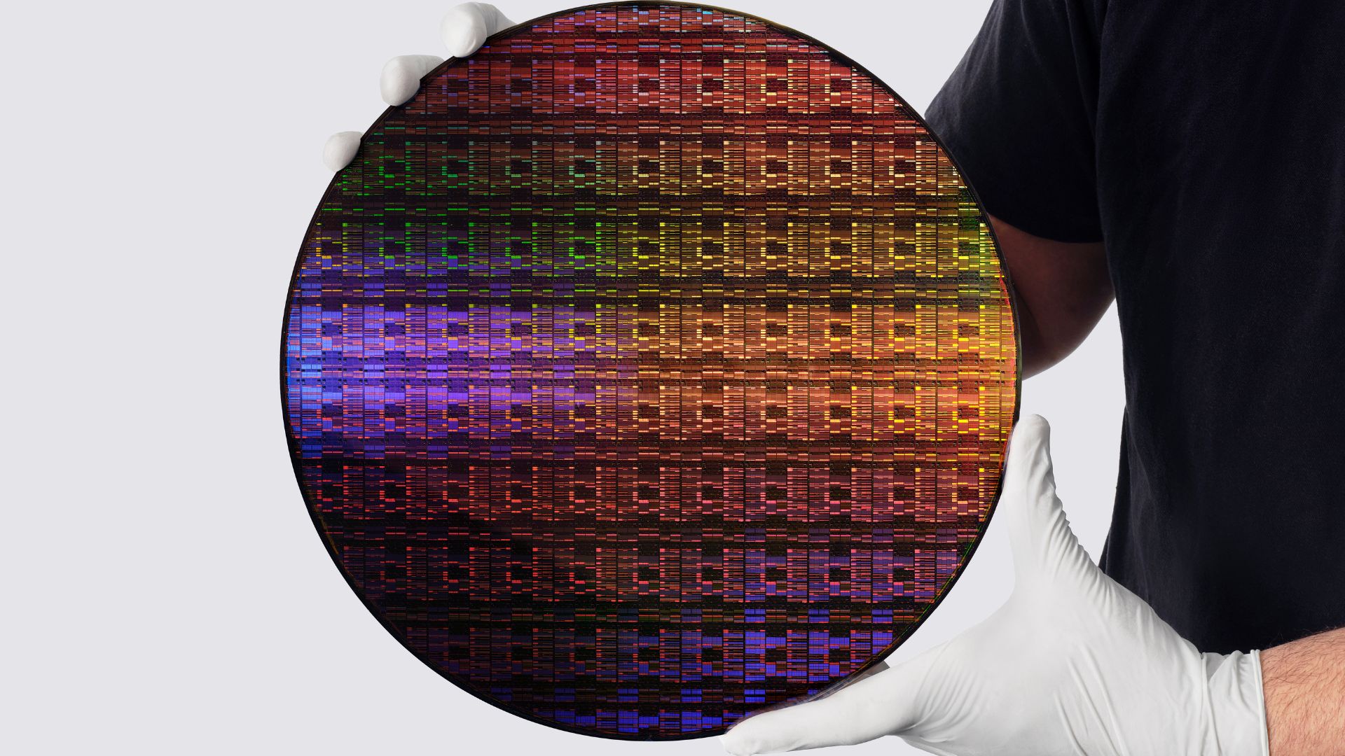
The chip is built on a 0.7-nanometer node, which is close to the size of an atom.
For years, the technology industry has been very concerned about what will happen when the chips can no longer be shrunk. The number of devices that rely on chips, from phones and cars to the data centers that hold the internet, all require a significant improvement in the number of chips that are available. IBM has found a way to make this possible.
From Flat to 3D
The company’s main innovation was a shift from flat to three-dimensional chips. Specifically, IBM created a design referred to as a nanostack. Rather than placing the components next to each other on the chip’s platform, IBM stacks them vertically.
As a result, IBM can fit 100 billion transistors into an area the size of a fingernail. That is nearly double the number of transistors in IBM’s previous chip model, which the company released in 2021. Moreover, the vertical chip design allows the company to use different materials on different layers of the chip, enabling transistors to run faster while consuming less power.
“IBM’s latest chip breakthrough marks a landmark moment in computing, pushing technology beyond the nanometer era to the scale of atoms. With our new nanostack architecture, we’re not just making smaller transistors, we’re reinventing how chips are built to deliver dramatically more power and energy efficiency,” said Jay Gambetta, Director of IBM Research and IBM Fellow. “This industry-first innovation continues IBM’s legacy of leading in next-generation technologies and sets the foundation for the next era of computing.”
Advertisement
What Does This Mean For Us?
This chip can deliver up to 50% higher performance while using 70% less energy than current 2-nanometer chips.
This will translate into better performance from laptops that run artificial intelligence applications, data centers could save money on their electricity bills, and devices will charge longer.
Building the Future
Unfortunately, this will not be available in stores anytime soon. The cost and difficulty of building technology on the atomic scale are considerable. However, according to IBM, it will be at least five years before these chips go into mass production.
IBM built the test chip at a facility in Albany, New York. Highly precise circuit printers etched the chip’s design into the silicon. Producing this chip required a significant investment of time and money. However, it does provide the technology industry with a head start on the future of chips over the next decade.