UC Berkeley is joining Applied Materials’ new EPIC Center in Silicon Valley. The goal is for students and faculty to work directly with industry experts to develop the materials needed for the future of AI computing.
Universities usually come up with the big ideas for new microchips. But those ideas often get stuck waiting because schools don’t have the massive, expensive equipment that big factories use. The EPIC Center gives these researchers access to full-scale industry tools to test their ideas faster and get them ready for the real world sooner.
A History of Building
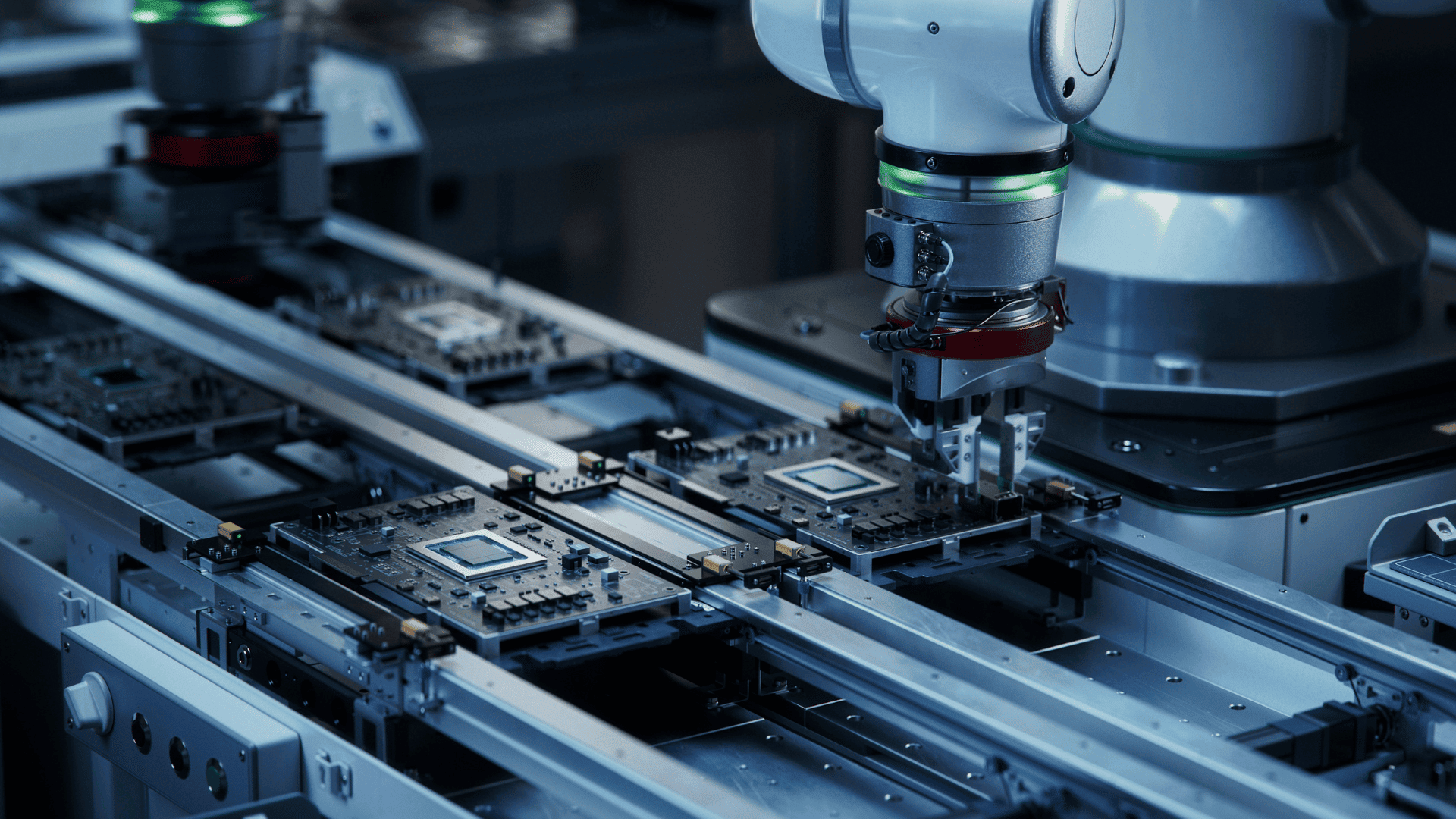
Back in 1962, UC Berkeley built the first university lab just for making integrated circuit prototypes. Since then, they helped create things like the SPICE circuit simulator and the FinFET 3D transistor.
Advertisement
Now, they are bringing that history to the EPIC Center, which opens in 2026. The facility is the largest U.S. investment in advanced semiconductor equipment research.
“The EPIC Center is designed to bring together the best minds from industry and academia in a high-velocity, manufacturing-relevant environment to dramatically accelerate the development and commercialization of next-generation semiconductor technologies,” Dr. Prabu Raja, President of the Semiconductor Products Group at Applied Materials, explained. “Few institutions have shaped modern chipmaking as profoundly as UC Berkeley. Expanding our research collaboration at the EPIC Center strengthens the lab-to-fab innovation pipeline and gives us a powerful platform for developing the semiconductor talent the industry will depend on for decades to come.”
Deepening Existing Ties
Applied Materials and UC Berkeley already share lab space and work together through groups like the Berkeley Emerging Technologies Research Center. A lot of Berkeley alumni also end up working at Applied Materials as engineers and managers. Both groups are right in Silicon Valley, which makes it easy to share ideas and equipment.
“Pioneering innovations by UC Berkeley researchers have enabled advancements in semiconductor chip technology, resulting in the exponential growth of computing that has ushered in the AI era,” Mark Asta, dean of UC Berkeley’s College of Engineering, said. “Applied Materials’ new EPIC Center in the heart of Silicon Valley aims to speed the translation of university inventions into commercial products by providing early access to cutting-edge, industrial-scale semiconductor process equipment and technologies. I look forward to advancing research and supporting new engineering talent through this R&D collaboration with Applied Materials.”
 Read Exclusive Stories
 Bookmark & Save Articles For Later